P- N JUNCTION DIODE P-N - Class 12 Physics Semiconductor Chapter
Diode or P-N Junction Theory Explained
Introduction
A diode is a fundamental component in electronics, widely used for its unidirectional current-carrying property. At the core of its operation lies the P-N junction—a boundary or interface between p-type and n-type semiconductors. Understanding the theory of the P-N junction, including forward and reverse biasing, depletion regions, and V-I characteristics, is crucial for anyone learning electronics or semiconductor physics.
This blog explains the theory behind the P-N junction and how diodes work under various conditions, with all the important parameters and equations included.
Table of Contents
What is a Diode ?
Formation of P-N Junction
Depletion Layer
Potential Barrier and Electric Field
Forward and Reverse Biasing
Forward Bias
Reverse Bias
V-I Characteristic of Diode
Ideal vs Practical Diode
Conclusion
What is a Diode?
A diode is a non-linear, active, and unidirectional device. It allows current to flow in one direction only, making it essential for rectification and signal conditioning applications.
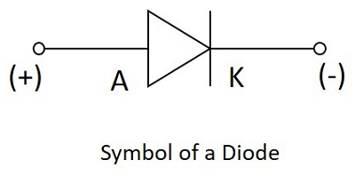
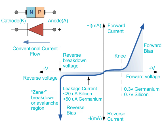
A p -n junction forms a popular Semiconductor device called p - n junction diode. It has two terminals, one electrode each from P region and n region hence called diode( d i Plus electrode). In the symbol of a diode and arrowhead indicates the conventional current direction when it is forward biased. Diode allows current to flow in only one direction.
Formation of P-N Junction
A P-N junction can be formed only when a bonding force is created between p-type and n-type semiconductors. Modern diodes are fabricated using:
Alloy junction technology
Growth in semiconductor processing
Exitarial methods
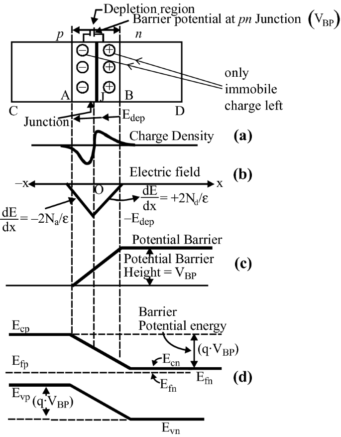
If donor impurities are introduced into one side and acceptors into the other side of a single crystal of a semiconductor , a PN junction is formed . The donor ion is represented by a plus sign because, after this impurity atom donates an electron it becomes a positive ion. The acceptor iron is indicated by a minus sign because after this atom accepts an electron , it becomes a negative ion .Initially there are only p type carriers to the left of the junction and only n type carriers to the night.
At the junction, electrons from the N-side diffuse into the P-side and recombine with holes, while holes move into the N-side and recombine with electrons. This movement of charge carriers forms a depletion region and establishes an internal electric field.
Depletion Layer
The depletion layer (also known as space charge region or transition region) is created due to diffusion of majority carriers across the junction.
Because there is a density gradient across the junction, holes will initially diffuse to the right across the junction, and electrons to the left. We see that the positive holes which neutralized the acceptor ions near the junction in the p type silicon have disappeared as a result of combination with electrons which have diffused across the junction. Similarly the Neutralizing electrons in the n Type Silicon have combined with the holes which have crossed the junction from the P material. The unneutralized ions in the neighborhood of the junction are referred to as uncovered charges. Since the region of the junction is depleted of mobile charges, it is called the depletion region.
Key points:
Mobile charge carriers in the depletion layer are zero.
It contains ions and covalent bonds or immobile charge particles.
Negative ions (acceptor ions) appear on the P-side.
Positive ions (donor ions) appear on the N-side.
Width of depletion layer (W) is inversely proportional to the square root of doping concentration:
W ∝ 1 / √(Doping Concentration)
Typical width: 0.1 to 1 μm (micrometer), average ~0.5 μm.
Potential Barrier and Electric Field
The space charge density is zero at the junction. It is positive to the right and negative to the left of the junction. This distribution constitutes an electrical dipole layer , giving rise to the electric lines of flux from right to left , corresponding to negative field intensity E . The field intensity curve is proportional to the integral of the charge density curve.
POTENTIAL :
The electrostatic potential variation in the depletion region is shown in above fig. and is negative integral of the function. The variation constitutes a potential energy barrier against the further diffusion of holes across the barrier . The form of the potential energy barrier against the flow of the electrons from the n side across the junction is also shown.
key points :
The potential barrier or contact potential is negative towards the P-side and positive towards the N-side.
For Ge diodes: 0.1 to 0.5 V (typical: 0.2 V)
For Si diodes: 0.6 to 0.9 V (typical: 0.7 V)
This induced voltage cannot be practically measured using a voltmeter.
Electric field intensity is maximum at the center of the junction.
Majority carriers face the potential barrier, while minority carriers are assisted.
Depletion layer opposes majority carriers but not minority carriers.
The electric field is zero outside the depletion layer.
Forward and Reverse Biasing
Let’s understand what happens when a diode is connected under forward or reverse bias.

First we will see WHAT IS BIASING :
Biasing of any electronic device means the application of external D.C voltage. A diode allows current to flow in only one direction . This is essentially controlled by way of biasing a diode . Depending upon the polarity of the D.C voltage externally applied to it , the biasing is being classified as forward and reverse biasing of a diode.
Forward Bias
A p-n junction is forward biased when a negative voltage is applied to the N-side and positive to the P-side.
when a diode is connected in forward bias, the negative terminal of the battery pushes the free electrons in the n region towards the junction . Similarly , the holes from p region is reppled by the positive terminal of the baterry and moves towards the junction.
If this external voltage becomes greater than the value of the potential barrier, approx. 0.7 volts for silicon and 0.3 volts for germanium, the potential barriers opposition will be overcome and current will start to flow. This is because the negative voltage pushes or repels electrons towards the junction giving them the energy to cross over and combine with the holes being pushed in the opposite direction towards the junction by the positive voltage. This results in a characteristics curve of zero current flowing up to this voltage point, called the "knee" on the static curves and then a high current flow through the diode with little increase in the external voltage.
Effects in forward bias:
Depletion layer width decreases
Potential barrier decreases
Current flows due to majority carriers
Diode Equation:
If = Io * (e^(Vd / n.Vt) - 1)
Where:
If: forward current
Io: reverse saturation current
Vd: voltage across diode
Vt: thermal voltage (≈26 mV at room temp)
n: ideality/recombination factor (1 to 2)
- Forward current (If ) of diode exponentially increases with voltage across the diode(
V D). In a forward bias diode forward current is due to majority carriers that are independent of temperature and majority carriers will be crossing the junction from higher concentration to lower concentration. Hence , forward current is diffussion current.- Forward current is independent of temperature.
- Forward current is derived in terms of minority carrier current.
Forward Voltage:
As, If ≈ Io (e^Vd/n.Vt)
therefore FORWARD VOLTAGE is given by ,
Vd ≈ n.Vt.ln(If / Io)
- from the above expression of forward voltage across diode ( Vd ), Vd ∝ Vt and Vd ∝ ln( 1 / Io ) . If temperature is 0 kelvin then threshold voltage ( Vt ) is equal to zero and at 300 kelvin , Vt is 26 mV. Therefore, reverse saturation current ( Io ) is more sensitive to temperature. Hence, as temperature increases forward voltage across diode ( Vd ) decreases.
As temperature increases, forward voltage (Vd) decreases.
- Cutin voltage/ knee voltage/ offset voltage / threshold voltage / breakdown voltage ( Vbr ) is the minimum forward voltage required for majority carrier to cross junction or for the flow of forward current .
- cutin voltage decreases with the temperature. For 1 degree C cutin voltage is reduced by 2.3 mv.
- In any type of P-N junction breakdown voltage is inversely proportional to doping concentration.
Cut-in voltage (threshold/knee voltage) decreases with temperature (~2.3 mV per °C).
Breakdown voltage is inversely proportional to doping concentration.
Reverse Bias
In reverse bias, positive voltage is applied to N-type and negative voltage to P-type.
Majority carriers are pulled away from the junction, widening the depletion layer.
when a diode is connected in reverse bias, the negative terminal of the battery attracts holes in the p region away from the junction. Similarly the electrons from the n region are attracted by the positive terminal of the battery and moves away from the junction . That's why in reverse bias the width of depletion layer is wide and so a very small minority charge carrier current flows across a reverse bias junction measured in microamperes, (μA).
 The net result is that the depletion layer grows wider due to a lack of electrons and holes and presents a high impedance path, almost an insulator.
 - The result is that a high potential barrier is created thus preventing current from flowing through the semiconductor material.
- This condition represents a high resistance value to the PN junction and practically zero current flows through the junction diode with an increase in bias voltage. However, a very small leakage current does flow through the junction which can be measured in microamperes, (μA).
- When P-N junction is reverse biased the width of the depletion layer increases and also the barrier height increases.
- In a reverse biased diode current is only due to the flow of minority carriers.
Effects in reverse bias:
High resistance path is created
Almost zero current flows
Only minority carriers contribute — this is drift current
Typical Io Values:
Temperature dependency:
- Reverse saturation current (Io) doubles for every 10 degree C , for 1 degree C Io approximately increases by 7%.
- Io is highly sensitive to temperatures,
Io(T2) = Io(T1) × 2^((T2–T1)/10) Amp
- Io flows from n side to p side.
- In a reverse biased diode, majority carriers will be moving away from the junction and therefore will not contribute any current.
- Reverse current is DRIFT CURRENT.
- In a reverse biased diode, the current is due to minority carriers and these minority charge carriers will be crossing the junction under the influence of electric field intensity. Hence, reverse current is drift current.
- when diode is reverse biased the reverse voltage must be always less than breakdown voltage of the device.
V-I Characteristics of Diode
Ideal Diode
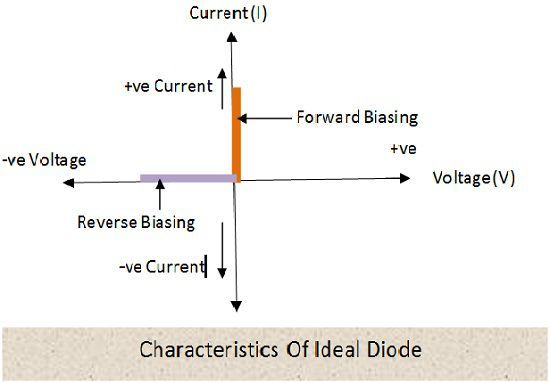
Forward biased: the ideal diode behaves like short circuit (Rf = 0)
Reverse biased: the ideal diode behaves like open circuit (Rr = ∞)
Practical Diode
- In forward biased condition as long as forward voltage is less than cutin voltage, there is no forward current so forward current is zero. Once forward voltage becomes greater than cut -in voltage, the forward current starts flowing. Once the depletion layer collapes at a particular value of forward voltage , the forward current increases drastically . The nature of the forward characteristics is exponential . The p-n junction offers small resistance in forward biased condition called forward resistance.
- The polarity of reverse voltage applied is opposite to that of forward voltage . Hence in practice reverse voltage is taken as negative . Similarly the reverse saturation current is due to the minority carriers and is opposite to the direction of forward current . Hence in practice reverse saturation current is also taken as negative. Hence the reverse characteristic is plotted in third quadrant .
- As reverse voltage is increased , reverse current increases initially , but after a certain voltage , the current remains constant equal to reverse saturation current though reverse voltage is increased .The p-n junction offers large resistance in the reverse biased condition called rverse resistance.
In forward bias ,diode Conducts after cut-in voltage
In reverse bias, blocks current except small leakage
Log If vs Vd gives a straight line plot
Important Note:
When solving circuits, if no resistance is given, replace a forward-biased diode with its cut-in voltage:
Ge diode: 0.2 V
Si diode: 0.7 V
Conclusion
The P-N junction diode is a cornerstone of modern electronics. Understanding how it functions under different biasing conditions, its depletion region behavior, and the mathematical expressions governing current and voltage helps in designing reliable circuits. Whether you're a student, an engineer, or an electronics enthusiast, mastering this concept will pave the way for deeper knowledge in semiconductor physics.


Comments
Post a Comment