Classification of Semiconductors – Class 12 Physics Notes with Examples
Understanding Semiconductors: Band Gaps, Types, and Doping
Introduction
A Semiconductor is a material whose conductivity lies between that of conductors and insulators.
Semiconductors play a central role in modern electronics. Their behavior depends heavily on factors such as energy band gaps, material purity, and temperature.
This blog presents a complete explanation of semiconductors, including classifications, intrinsic and extrinsic types, and how doping affects their properties.
Table of Contents
Classification of Semiconductors
Energy Band Gap
Direct vs Indirect Band Gap Semiconductors
Intrinsic Semiconductors
Doping in Semiconductors
Extrinsic Semiconductors
Effect of Temperature on Conductivity
N-Type Semiconductors
P-Type Semiconductors
Basic Numerical Questions
Classification of Semiconductors
Semiconductors are classified based on:
-
Energy band gap type:
-
Direct band gap semiconductors
-
Indirect band gap semiconductors
-
-
Material purity:
-
Intrinsic semiconductors
-
Extrinsic semiconductors
-
Energy Band Gap
Now let's understand BAND GAP in semiconductors, metals and insulators one by one.
The energy band gap is the energy difference between the valence band, where electrons are bound and not free to move, and the conduction band, where electrons are free to move.

This gap determine the behaviour of NATURAL ELEMENTS in term of electrical and optical properties.
In the band gap (also called the energy gap), no charge carriers can stay. Electrons either stay in the valence band or gain energy to jump to the conduction band and vice versa. That's why the band gap is also called the forbidden energy band, meaning it is a region where no electrons can exist — it is prohibited or unacceptable for electron presence.
When an electron gains enough energy to cross this energy gap from the valence band to the conduction band, the semiconductor begins to conduct electricity.
Temperature Dependence of the Energy Gap
The energy gap is temperature-dependent. It is inversely proportional to temperature because as temperature increases, the energy gap decreases; as temperature decreases, the energy gap increases.
The expression for energy gap is,
Eg(T) = Eg0 - 𝜷0 . T eV , where 𝜷0 is material constant
Eg0 energy gap at 0 K
FOR Ge Eg(T) = 0.785 - 2.2 X 10^-4 . T
FOR Si Eg(T) = 1.21 - 3.6 X 10^-4 . T
For example:
At 0 K, silicon has an energy gap of 1.21 eV, and germanium has 0.785 eV.
At 300 K, silicon has an energy gap of 1.1 eV, and germanium has 0.72 eV.
From this, we understand that as temperature increases, the energy gap decreases in semiconductors.
Also, since overlapping between the valence band and conduction band is directly proportional to temperature, the overlap increases with rising temperature. This means that as temperature increases, electrons gain enough energy to cross the band gap more easily.
In a semiconductor energy band gap is around one electron volt or 0.7 electron volt to
1.3 electron volt.
From the below fig. we can see the ENERGY BAND DIAGRAM FOR SEMICONDUCTORS AT 0 K & 300 K,

At zero kelvin temperature in semiconductors the valence band is filled with charge carriers
and the conduction band is empty so at zero Kelvin all the semiconductors are insulators.
As temperature increases to room temperature that is at 300 Kelvin charge Carriers are
created ,holes in the valence band and electrons in conduction band and there will be
conductivity in the semiconductor.
Key Points to Note :
- If the energy gap is large, the semiconductor is more suitable for high-temperature applications.
- Compared to germanium, silicon is more suitable for high-temperature usage due to its larger energy gap.
- As temperature increases, the atoms in the semiconductor vibrate more intensely due to thermal energy, which causes the energy gap to slightly decrease.
- In the forbidden energy gap, electrons are prohibited from staying. This rule is valid for all natural elements including metals, semiconductors, and insulators.
Now take a look about energy band gap in METALS / CONDUCTORS,

In metals at 0 K the energy gap is zero i.e no band gap exists between valance and conduction band. Therefore, in metals free electrons that are independent of temperature are often available even at 0 K. Hence , metal is a good conductor of current , even at 0 k .
As temperature increases to room temperature i.e at 300 K , the overlapping of valance band and conduction band increases with temperature.
Lastly , if we talk about the ENERGY GAP FOR INSULATORS ,

as we have seen from the above figure that is ENERGY GAP DIAGRAM FOR INSULATOR,
the energy gap in insulators is very large it is greater than 5 eV and because of this the conduction band remains empty as charge carriers are unable to cross band gap to reach there from valence band . Hence , all insulators are bad conductors of current .
example of insulators are mica , ceramic , bakelite , porcelain , diamond , rubber , pvc , glass , plastic.
Direct vs Indirect Band Gap Semiconductors
Direct Band Gap Semiconductors
In direct band gap semiconductors during the recombination majority of falling electrons will be directly falling from conduction band to valence band and thereby will be releasing the energy in the form of light , but very few electrons falling electrons gets collided with the crystal of the atom and these crystals will be absorbing the energy that they dissipate in the form of light
As the energy is released directly in the form of light by the falling electrons , hence the name of these semiconductors is direct band gap semiconductor.
When free electrons pair with holes it's called recombination .During the recombination free electrons and hole will disappear and a covalent bond will be formed ,as during the recombination the free electrons
will be falling from the conduction band to the valence band to combine with the hole and the energy will be released both in the form of heat and light .
In direct band gap semiconductors most of the energy will be released in the form of light.
In direct band gap semiconductors the direction of falling electrons remains unchanged but there is slight change in momentum and the energy of falling electrons changes in terms of kinetic and potential energy . The Carrier lifetime i.e the interval of time from breaking of covalent bond until its recombination is small.
Examples : GaAs, GaN, GaSb, ZnS, CdS, CdSe, InP, InAs
Indirect Band Gap Semiconductors
In indirect band gap semiconductors during the recombination most of the falling electrons from conduction band to valence band get collided with the crystals of the atom and these crystals will be absorbing the energy and get heated up and they release energy in the form of heat. But very few falling electrons may be escaping the collision and they will be directly falling from conduction band to valence band and releasing the energy in the form of light (99 % high & 1% low). Most of the falling electrons will be releasing the energy indirectly to the crystal of the atom in the form of heat and hence the name of these semiconductors is indirect band gap semiconductors. So , as we have observed, most of the energy will be released in the form of heat.
In indirect band gap semiconductors the direction of falling electrons slightly changes due to the number of collisions with the crystal of the atoms and also there is slight change in momentum and the energy of falling electrons changes both in terms of kinetic and potential energy .The Carrier lifetime of indirect band gap semiconductors as compared to direct band gap semiconductors is larger.
Examples : Ge, Si, AlP, PbS, AlAs, PbSe, AlSb, GaP
Intrinsic Semiconductors
A sample of semiconductor in its purest form is called an intrinsic semiconductor or in other words we can say , an intrinsic semiconductor is a pure or non-degenerated semiconductor with no impurities or doping.
The outermost shell of an intrinsic semiconductor like silicon has only four electrons. Each of these four electrons forms a bond with another valance electrons of neighbouring atoms.
At room temperature, the number of valance electrons absorbs the thermal energy, due to which they break the covalanet bond and drift to conduction band.When a valance electron jumps or drifts from valence to conduction band breaking a covalent bond , a vacancy is created in the broken covalent bond . Such a vacancy is called hole. Whenever an electron becomes free , the corresponding hole gets generated . So , free electrons and holes get generated in pairs . The concentration of free elcetrons and holes is always equal in an intrinsic semiconductor.
In intrinsic semiconductor carrier concentration means electron concentration and hole concentration .
The disadvantage of intrinsic semiconductor is that the conductivity is very small, this is due to the smaller value of intrinsic carrier concentration both in Ge and Si.
Key Characteristics of INTRINSIC SEMICONDUCTORS :
At T=0 K
- the maximum number of valence electrons are 8.
- all valence electrons are in perfect covalent bonding.
- intrinsic semiconductor will work as a perfect insulator .
At T=300 K
- equal number of electrons and holes are present in valence band and conduction band just because of equal number of breakings in pure semiconductor material atom, that's why n = p = i (intrinsic carrier concentration) .
- when a covalent bond is broken it will create one electron and one hole ( the electron jumps from valence to conduction band and becomes free electron but the hole will remain in the valance band).
- hole is defined as the deficiency of an electron in broken covalent bond.
- hole is a carrier of current and is associated with positive charge.
- because of opposite polarities electron and hole always move in the opposite direction but they contributes current in the same direction.
- note: current direction is opposite to the flow of electrons or in the direction of hole flow.
- in a semiconductor the free elecrons will be moving in the conduction band and will contribute the current but at the same time holes will be moving in the valence band in the opposite direction , so that I = In + Ip .
Conductivity Equation of intrinsic semiconductor :
As the conductivity of a semiconductor is given by ,
σ = n.q. μe + p.q.μh mho/m
but in intrinsic semiconductor n = p = ni
therefore ,
σ = q.ni (μe+μh) ----------(a)
σ ∝ ni
but ni ∝ T^1.5
∴ σ ∝ T^1.5 therefore as temperature increases conductivity increases in intrinsic semiconductor .
Doping in Semiconductors
Doping is the process of adding impurities to a pure semiconductor .
Effects of Doping
-
Doping Increases the number of charge carriers, increasing conductivity.
When impurity atoms are suddenly introduced in the semiconductor , at first the conductivity slightly decreases (because the mean path (average path) of electrons and holes slightly decreases), and then the conductivity increases with the doping.
-
Doping Slightly decreases mobility of charge carriers due to lattice scattering.
-
Dopants are usually from group III (trivalent) or group V (pentavalent) elements because the properties of I , II , III group is different from IV group.
Dopant Types
-
Trivalent / Acceptor: B, Al, Ga, In
-
Pentavalent / Donor: P, As, Sb, Bi
Doping Levels
-
Lightly doped: 1 : 10 ^ 11
-
Moderately doped: 1 : ( 10 ^ 6 to 10 ^ 8) P -N [ 1: 10^6 means impurity atom for 10^6 number of atoms].
-
Highly doped: 1 : 10 ^ 3
A Highly doped semiconductors may :
-
Exhibit metallic properties i.e have high conductivity.
-
Show positive temperature coefficients.
-
Can become unipolar.
Note: The minimum impurity required to convert intrinsic to extrinsic semiconductor is 1 : 10 ^ 8.
Extrinsic Semiconductors
The process of adding other materials to the crystal of intrinsic semiconductors to improve its conductivity is called doping as we have discussed above and doped semiconductor material is called Extrinsic semiconductors these are also known as:
-
Doped semiconductors
-
Impurity semiconductors
-
Artificial semiconductors
-
De-generated or compensated semiconductors
Carrier Behavior
-
Majority carrier concentration increases with doping and is almost independent of temperature.
-
Minority carrier concentration decreases with doping and increases with temperature.
Effect of Temperature on Conductivity of EXTRINSIC SEMICONDUCTOR:
|
|---|
TYPES OF EXTRINSIC SEMICONDUCTOS :
1. N -TYPE SEMICONDUCTOR ( DONAR)
2. P -TYPE SEMICONDUCTOR (ACCEPTOR)
N-Type extrinsic semiconductors
N -Type semiconductors are formed by adding pentavalent impurity to a group IV element like silicon or germanium.
In n type the impurity is pentavalent having five valence electrons is added to a pure semiconductor having four valence electrons (silicon or germanium).Such impurities are known as donor impurities because they donate free electrons to semiconductor crystal.
In n- type semiconductor every impurity atom will be donating one electron into the conduction band. Hence , N-type is also called as donar type.
At T = 0 K
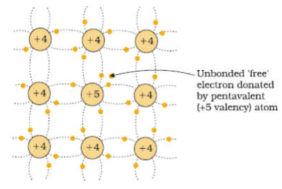
- At T = 0 K , the 5th electron of all the impurity atoms are existing in the donar energy level that exists just below the conduction band.The 5 th electron / excess electron / parent electron is not a free electron , its bonded electron with impurity atom .The additional energy required to detatch the 5th electron from its orbit is equal to 0.01 eV for Ge and 0.05 eV for Si.
- Donar energy level denotes the energy level of all the pentavalent atoms added to the pure semiconductor .
- Energy gap is more because of pentavalent impurity.This gap depends on inter-atomic spacing of the element.
- N-type semiconductor at T = 0 K will be working as a perfect insulator because all valence electrons are in a perfect covalent bonding.
At T = 300 K

- In n- type semiconductor , as temperature is increasing the 5th electron will be moving from donar energy level into conduction band and also due to temperature a large number of covalent bands will be broken creating equal number of electrons and holes and these electrons will be shifted into the conduction band so that the electron concentration in conduction band is far greater than hole concentration in valence band. Hence , electrons are majority carriers and holes are minority carriers .
- At T = 300 K (ROOM TEMPERATURE) donar level ionisation is completed i.e all the impurity atoms shifted to conduction band. i.e electrons moves from donar energy level (Nd ) to conduction band or if T > 300 K bonds will be broken in valance band and electrons jumps from valance band to conduction band creating holes.
- Donar level ionisation means moving of electrons from donar energy level (Nd ) to conduction band.
- Donar level ionisation increases with temperature.
- In n- type semiconductor , current is predominately created by the flow of electron.
Key Equations
-
Law of neutrality:
➡According to the law of electrical nutrality ,
Nd + p =Na + n
In n-type semiconductor , Na = 0
∴ n =Nd + p
since n >> p ,
∴ n ≈ Nd where Nd is called donar concentration and indicates the actual number of pentavalent atoms added to the pure semiconductor .
Nd = TOTAL NO. OF ATOMS PER VOLUME X IMPURITY RATIO
-
Conductivity:
The conductivity of N-Type semiconductor is ,
σ = n.q. μe + p.q.μh mho/cm
σ ≈ n.q. μe or σ ≈ Nd.q. μe mho/cm
-
Carrier relation:
The condition for N-Type semiconductor is ,
n > ni , p < ni
In n- type semiconductor, as electron concentration increases above INTRINSIC CARRIER CONCENTRATION (ni ), the hole concentration falls below ni (eta i) and this is due to a large number of recombinations.
P-Type Extrinsic Semiconductors
Formed by adding trivalent impurity to a group IV element.When a small amount of trivalent impurity is doped pure semiconductor, it becomes p-type semi-conductor.
In a pure semiconductor (germanium) having 4 valence electrons, if a trivalent impurity (boron) having. '3' valence electrons is added, then 3 valence electrons of trivalent impurity form a covalent bond with three valence electrons of germanium.The fourth valence electron of Ge atom is unable to form a covalent bond. The incomplete covalent bond is being short of one electron. This missing electron is called a hole.
Every trivalent impurity atom contributes one hole in addition to thermally generated electron - hole pairs. Therefore, number of holes is more than number of electrons.
A very small amount of energy is needed for an electron to enter acceptor energy level from valence band. Thus, a hole is generated in the valence band corresponding to each ionised acceptor.

At T = 0 K

- P-type semiconductor at T = 0 K will behave as an insulator.
-
The Acceptor energy level exists just above the valence band.Acceptor energy level denotes the energy level of all the trivalent impurities added to the pure semiconductor .
-
At 0 K , there are No free carriers therefore behaves as an insulator.
At T = 300 K

- In P-type semiconductor every impurity atom will be receiving one electron to complete its covalent bonding. Therefore , p type is also called as acceptor.
- As temperature increases , due to the thermal energy a large number of covalent bonds will be broken creating equal number of electrons and holes. Most of these electrons will be moving from valence band to acceptor energy level for bonding and very few electrons will be moving from valence band to conduction band , so that the hole concentration in valence band is far greater than electron concentration in the conduction band. Hence , majority carriers are holes and minority carriers are electrons .
- In P-type semiconductor current is dominated by holes .
Key Equations
-
Law of neutrality:
According to the law of electrical nutrality ,
Nd + p = Na + n
In p-type semiconductor , Nd = 0
∴ p = Na + n
since p >> n or Na >> n
∴ p ≈ Na where Na is called acceptor concentration and indicates the actual number of trivalent atoms added to the pure semiconductor .
Na = TOTAL NO. OF ATOMS PER VOLUME X IMPURITY RATIO
Conductivity:
The conductivity of P-Type semiconductor is ,
- σ = n.q. μe + p.q.μh mho/cm
- σ ≈ p .q. μh or σ ≈ Na. q. μh mho/cm
-
Carrier relation:
The condition for P-Type semiconductor is ,
p > ni , n < ni
In P-type semiconductor , as hole concentration increases above INTRINSIC CARRIER CONCENTRATION (ni ), the electron concentration falls below ni (eta i) and this is due to bondings. But in N-type semiconductor this is due to a large number of recombinations.
NUMERICAL PROBLEMS BASED ON ABOVE THEORY:
- FIND INTRINSIC CONDUCTIVITY AND INTRINSIC RESISTIVITY AT ROOM TEMPERATURE. ASSUME ni=2.5 X 10^13 atoms / cm^3 , electron mobility = 3800 cm^2/v-sec, hole mobility = 1800 cm^2/v-sec .
- FIND THE CONDUCTIVITY & RESISTIVITY OF PURE SILICON AT ROOM TEMPERATURE. ASSUME ni= 1.5 X 10^10 atoms / cm^3 , electron mobility = 1300 cm^2/v-sec, hole mobility = 500 cm^2/v-sec .
- A PURE SEMICONDUCTOR (Ge) IS DOPED WITH DONAR IMPURITIES TO THE EXTENT OF 1: 10 ^7 . CALCULATE
- DONAR CONCENTRATION.
- CONCENTRATION OF ELECTRONS & HOLES.
- CONDUCTIVITY & RESISTIVITY OF DOPED SEMICONDUCTOR
- HOW MANY TIMES THE CONDUCTIVITY IS INCREASED DUE TO DOPING.
Conclusion
Understanding how semiconductors behave based on their band gaps, doping levels, and temperature responses is essential for designing reliable electronic components. Whether working with intrinsic or extrinsic materials, knowing their conductivity mechanisms helps optimize performance in real-world applications.


Comments
Post a Comment